

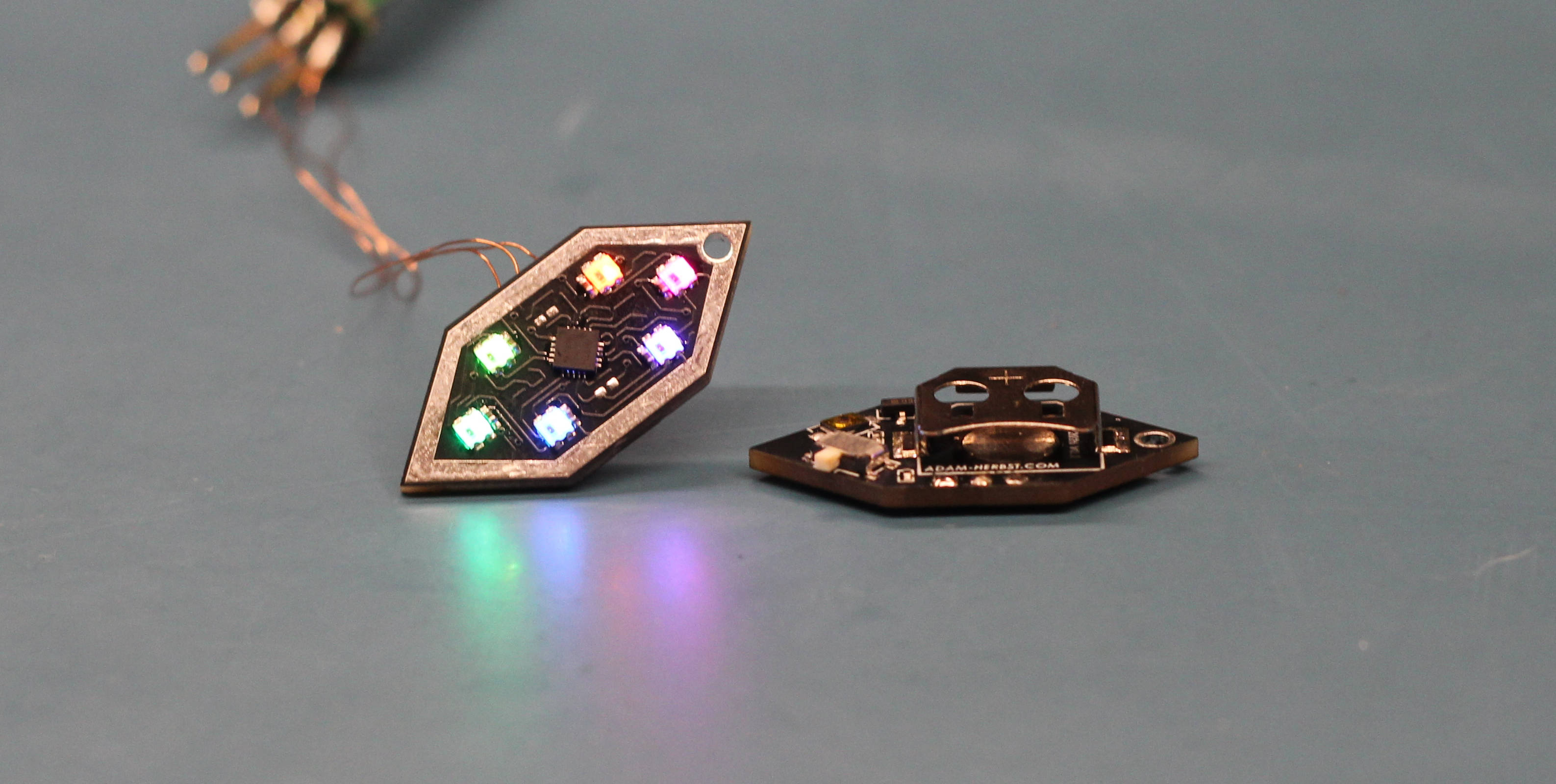
After getting a ridiculously good deal on a microscope, I was keen to try out some smaller PCB designs. Naturally, making earrings seemed to be the perfect challenge. Two challenges for this project were fitting everything onto a tiny board and optimizing the ATtiny to draw the least amount of current possible and still be functional, allowing for a good battery life given the tiny battery.
Some design considerations were to have a single button that depending on the duration it was held down, would change the brightness or the pattern currently being displayed. An analogue pin connected to VBAT to monitor the voltage level of the battery. On start up of the chip, it could flash a certain colour to inform the user how much battery life is left. Having a PFET in series with the VBAT solved the possibility of a user incorrectly placing the CR1220 coin cell battery back to front. Even though there is a "+" symbol on the holder, better safe than sorry.
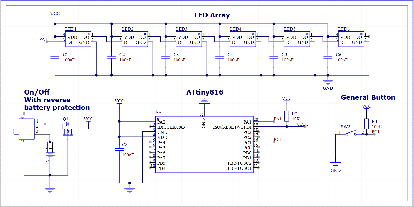
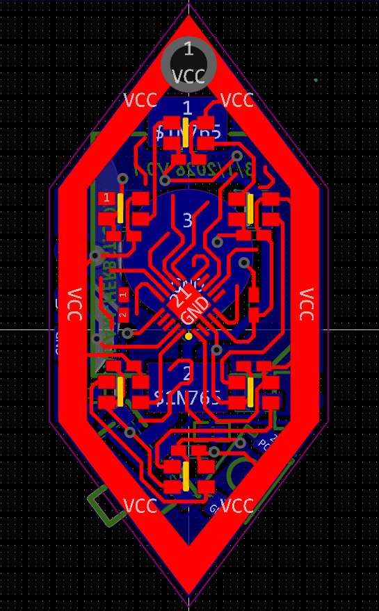
When designing prototypes, its easier to just accept the fact that the first version will instantly need better design considerations, let alone seeing if its wired correctly, it worked perfectly for this design. Just some alterations in the hole that seats the earring hook needed to be changed.
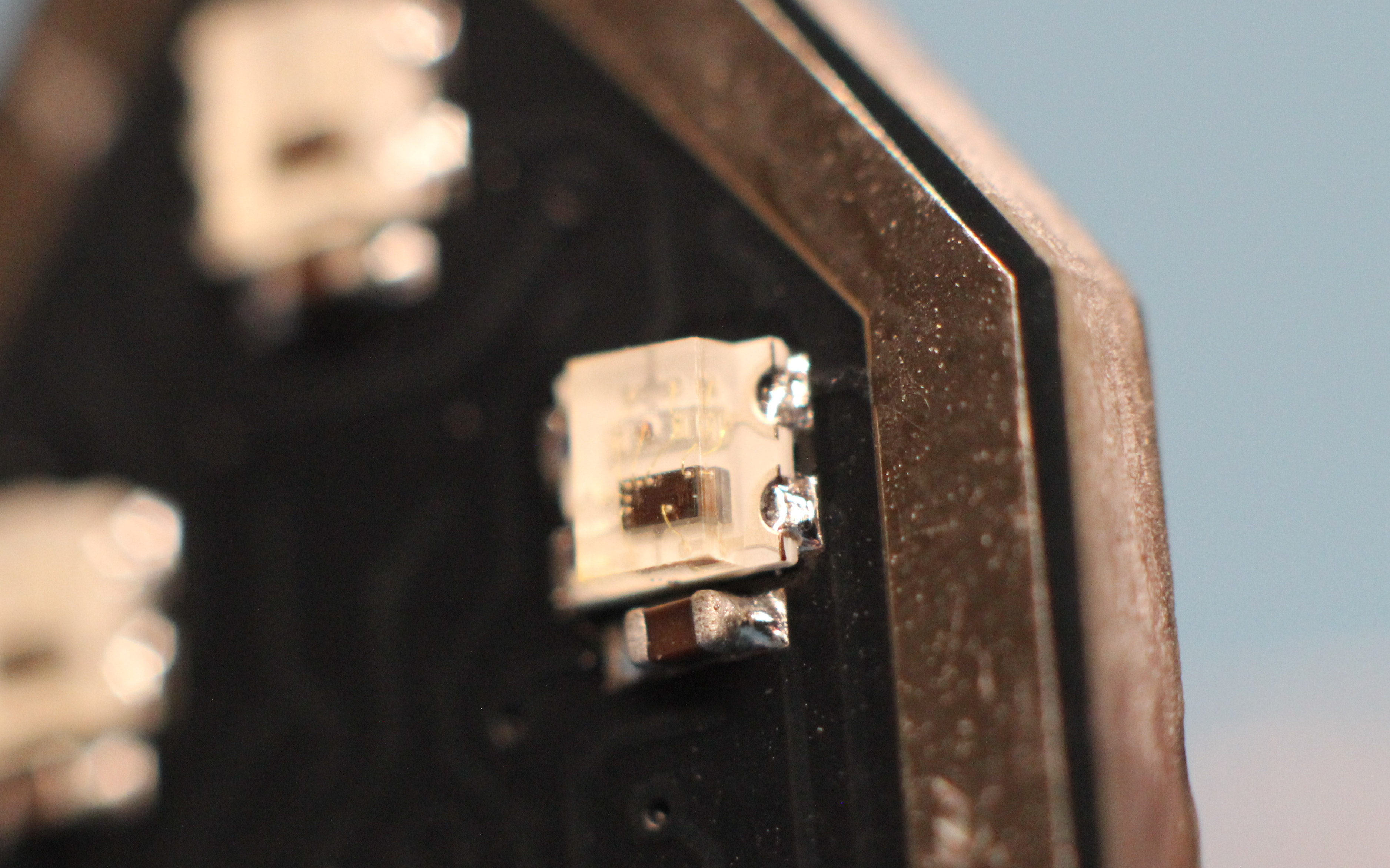
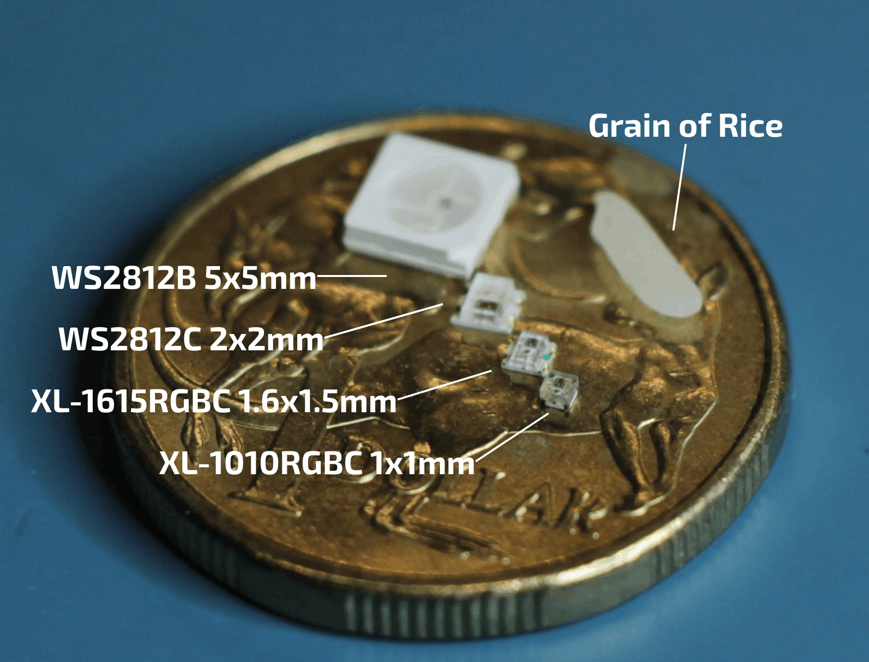
This designed used the WS2812C LEDS, but my second revision is going to use the XL-1010RGC LEDS, to give it that cool factor of just how small the components can get.
With each LED having a max power consumption of 60mA (20mA per channel) and the ATtiny816 having a power consumption of 8mA, I had to significantly reduce the power consumption in order to have a lasting battery life. The CR1220 battery has a capacity for 38mAh. Perhaps the easiest solution was to set the brightness from 100% down to around 5%. This was always intended as you want the earrings to be subtle in nature. With a brightness of 4%, the PCB was still drawing around 8.12mA.
An even better method to reducing energy consumption was to periodically turn on the LEDS for a fraction of the time and then turn them off and put the MCU into deep sleep. Deep sleep on the ATtiny816 was measured at 221μA, not too bad. Another solution was to reduce the clock speed of the MCU. Due to the single wire protocol of the LEDS, the MCU needed to have a timing accuracy of 220ns, this put a floor of around 4.5MHz for clock speed. It turns out that there is parasitic current draw when the LED's are on the board, with a single LED drawing 300μA at 3.3V in idle. I put a NFET in series with the LED's VDD and ground, therefore when in deep sleep, the LED's were physcially disconnected solving the unwanted current draw.
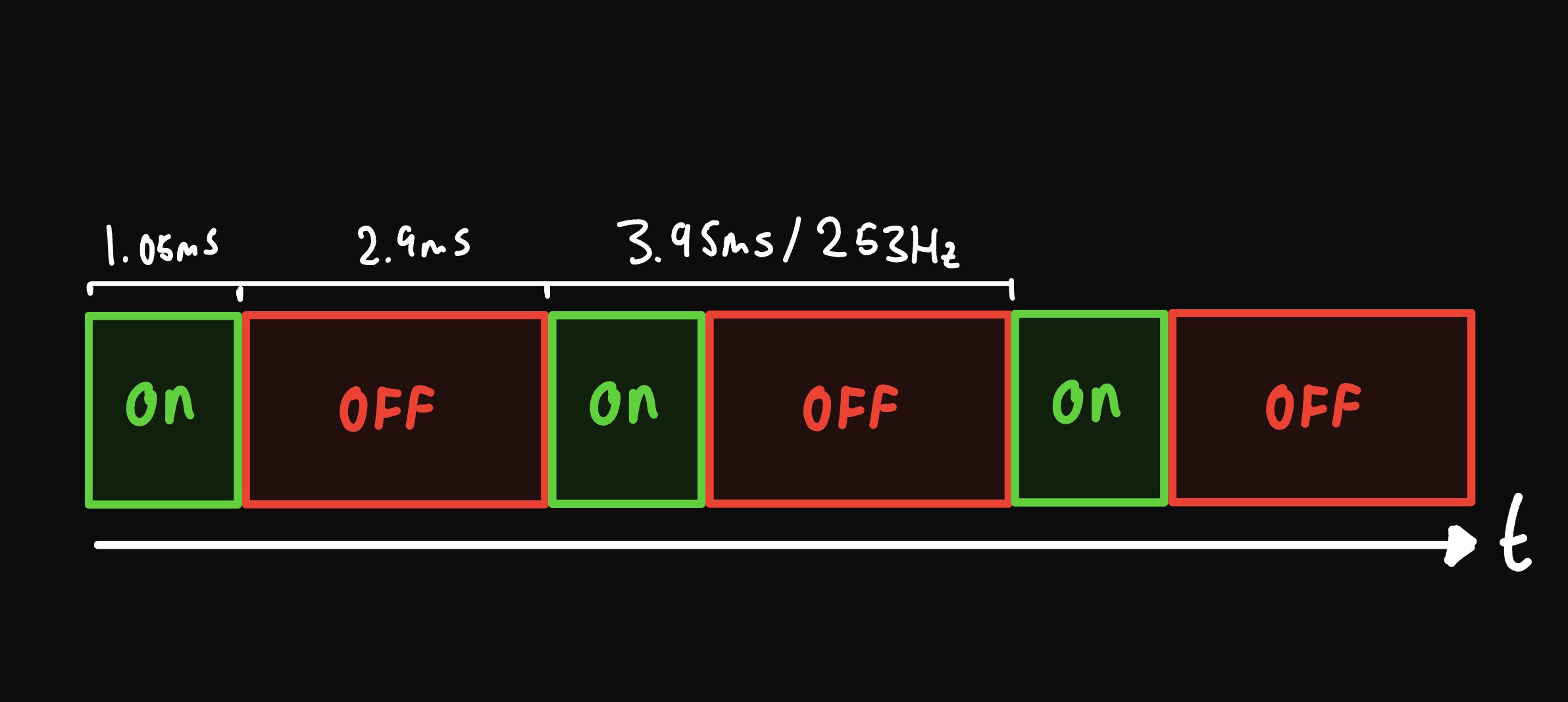
However, there is a trade off when reducing clock speed, the MCU spends more time processing and not sleeping. If you had say a 32MHz processor instead of the 16MHz in the ATtiny, ideally it should take half the time to run through the code updating the LEDs and vice versa. So higher clock chip consumes more current, but is awake for less time, I couldn't be bothered finding out a balance for the Atmel, as there's other MCU's specifically designed for low power. Here is a visual of the ATtiny wake and sleep times. It was awake for only 36% of the time, and the refresh rate of the LEDs were 253Hz.
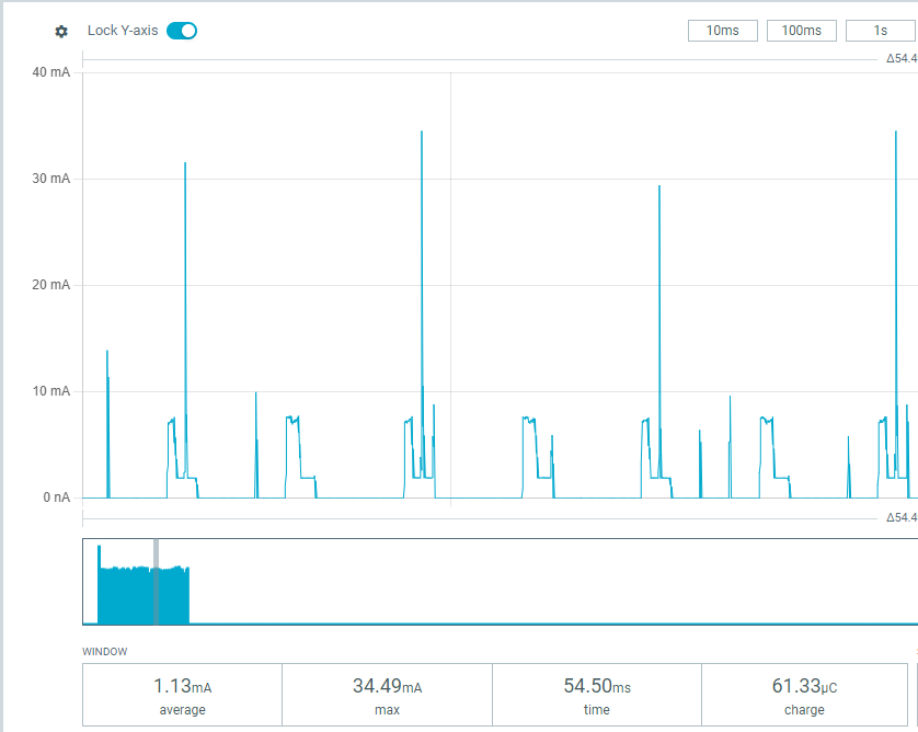

If you are doing any sort of power consumption testing, you need to get a Nordic Power Profiler Kit II, it is easily worth every cent. I hooked up the earring and as you can see it turns on, then off every 4ms. With an average current of 1.13mA. However, due to the weird spikes of current in which only last about 0.00001 seconds, it seems that this is too much for the CR1220. Well, even the average 1.13mA current consumption seems to ruin the battery as its 10 times the rated continuous current draw. The larger CR2032 battery works, however that is too large.
This left two paths, find an MCU that is specifically designed for low current draw, or find a different sort of battery. I think I'm going to do both, I would like to move away from Atmel chips and into the more industrious STM32's. I have ordered some 10105 LiPo batteries, those which are used in wireless earbuds. The good news about switching to LiPo's will be that the earrings are going to be rechargable.
The second version took alot more time. I wanted the earrings to be a product rather than a one-off design, which perhaps made all the difference and I had to start over from scratch. I needed a way to recharge them, something simple and easy, so that also meant designing a charging station. Below shows a couple of the PCB iterations, with all the soldered jumper wires as I continued to improve the design.
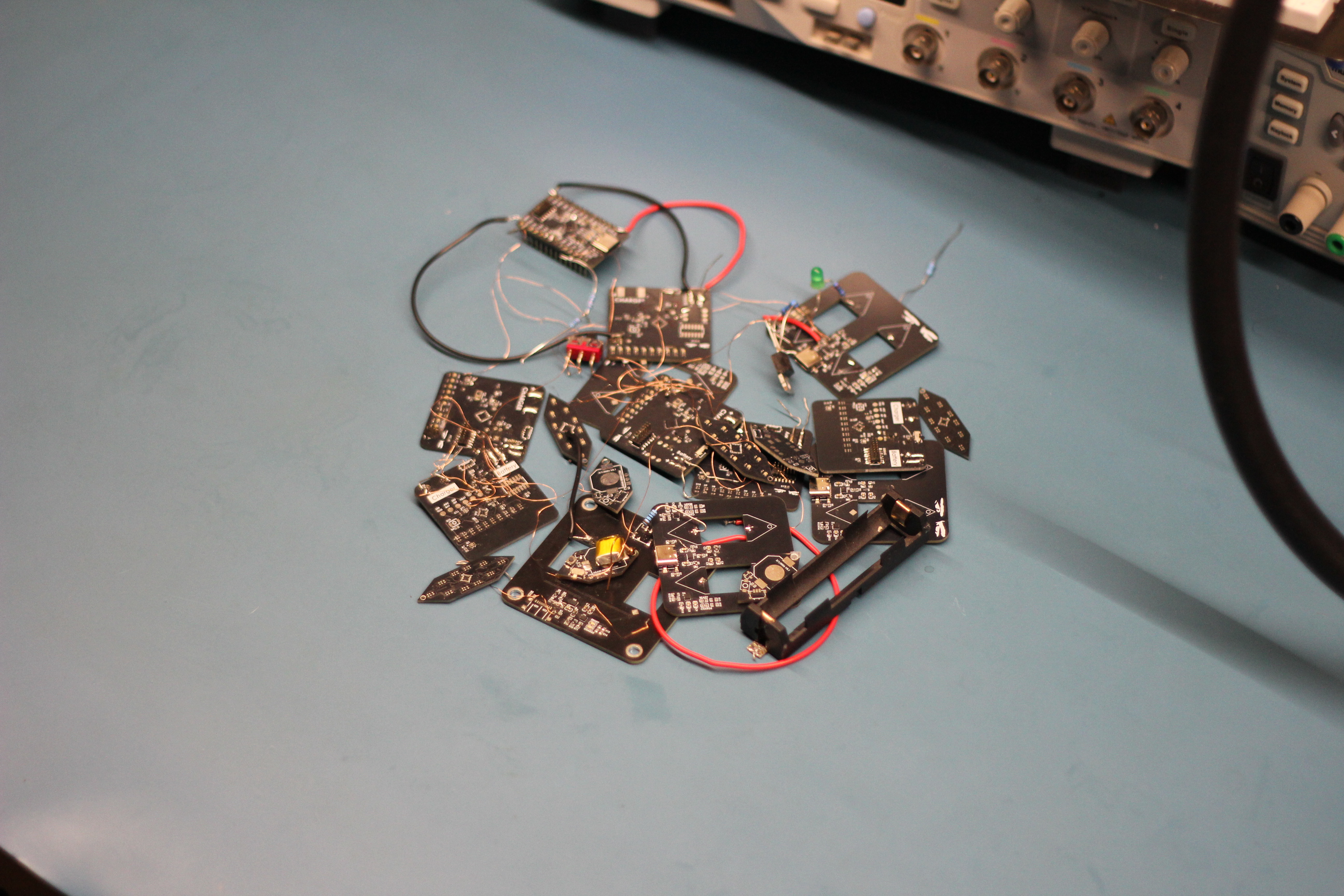
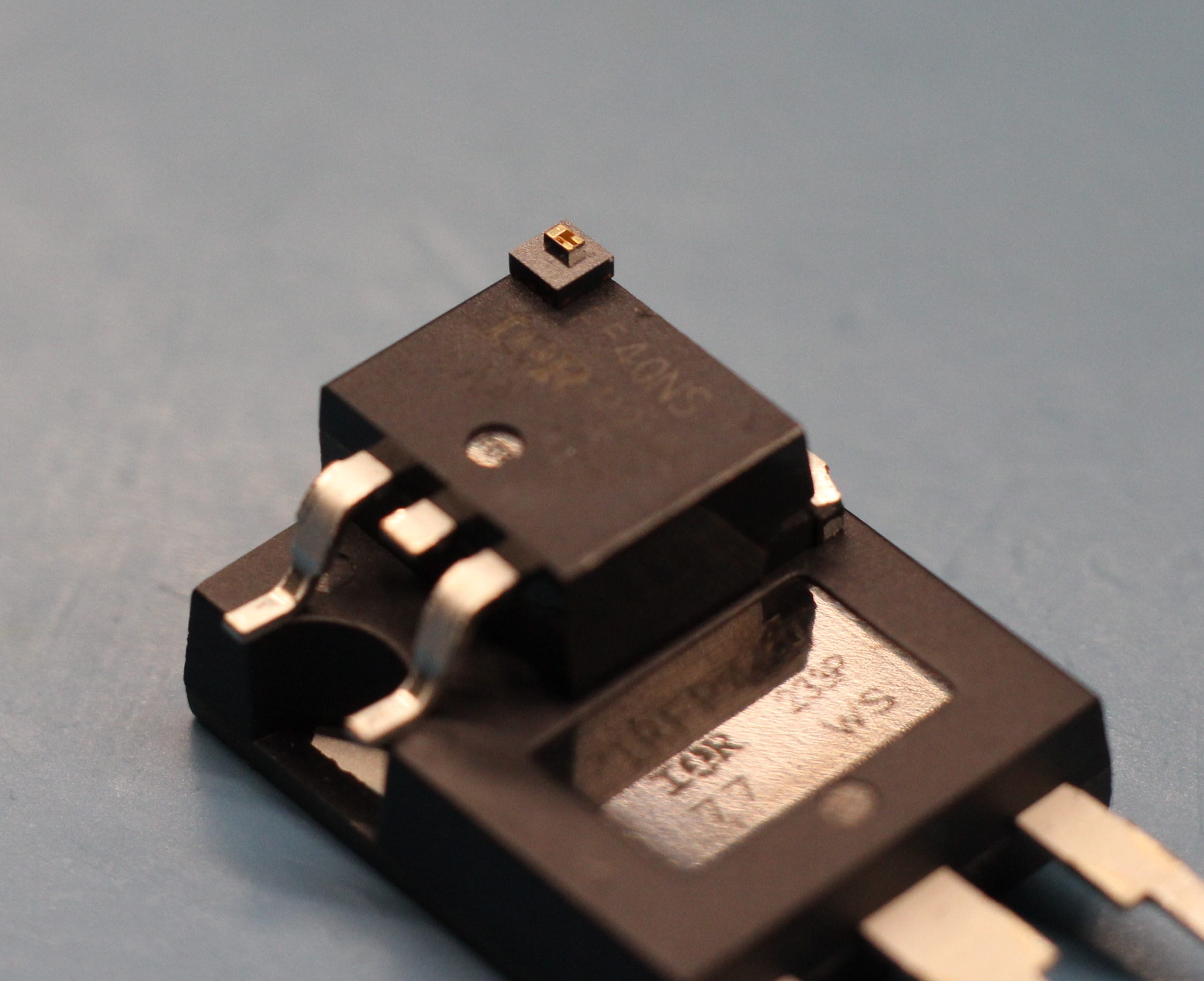
I went even smaller on the components, Ti offers MOSFETS in a 'Picostar-3' package (1x0.6mm), The smallest neopixels XL-1010RGBC (1x1mm).
Both the earrings and the base station needed to be designed at the same time. Starting off with the base station. I took inspiration from how Apple's AirPods work. The battery management side would all take place on the charging station. the station has a 250mAh LiPo battery, which can be charged via USB-C. This allows the earrings to be charged multipled times before needing to recharge the base station itself.
It turned out that making the charging station was harder than the earrings themselves. I used Ti BQ25180 and BQ25170 IC's for battery management. Each earring has a dedicated charging port. With the LiPo on the earring being only 25mAh, in order to safely charge it required max current of about 10mAh. I orginally wanted the station to be fully analogue, Making circuitry that would detect the earring's voltage level, and pull the BQ25170 into sleep mode, helping the standby current of the station itself. As well having the battery level indicator of the station display when turn on.
This required lots of additional components, op-amps and stuff, which in the end was more expensive than using a cheap microcontroller. Using a MCU instead saved me alot more time, and was easier to implement.
.jpg)
The station also had to be aesthetically pleasing, given mostly EE's would want this product. So I used a QFN packaging on all IC's. Rotating them on an angle gives and placing the components in a symmetrical orientation really gives the board a clean look. If you really want to have a modern looking PCB, QFN is the way to go. Through hole just looks ugly and outdated, and packages with legs (SOT, SOIC, QFP, etc) still aren't as clean looking as QFN. The only downside is you pretty much need breakout boards for everything as well as decent soldering skills, its really difficuit to diagnose solder connections on QFN IC's.
One of the hardest parts of the design was finding a way to connect the earrings to the base station. The small size of the earring meant I really couldn't't put any sort of connector on it. I went with the same method as Apple AirPods with magnets. That was anything but straight forward. Soldering magnets onto pads would heat the magnets up and they would lose their magnetism. You can buy electrically conductive glue / epoxy, which is infused with silver, but its extremely expensive at about $100 for 3mL! I'm going to be experimenting with ultra low temperature solder, as well as magnets with higher operating temperatures .